NerdpleXT
The mother of all (cheap'n complex) NXT I2C sensor port multiplexers. Supports I2C, A/D and 9V supply.
Features:
- supports up to 4 (different) 3.3V devices on one sensor port
- I2C support
- pin 1 A/D channel multiplexing support
- 2 switchable 9V supplies for output A+B or C+D
- allows mixed mode operation (analog/I2C)
- comes in 3 variants:
- N erd: 4 channel I2C multiplexing, A/D multiplexing, 9V support
- X tended: above without A/D multiplexing capability
- T oddler: I2C multiplexing, only
Will it work with every Lego/HiTechnic/Whatever sensor out there?
No, and it was never intended supporting any of them (simply because I don't use anything else
but the NXT itself)... Only for my own stuff ;-)
But all I2C sensors, including those which need a 9V supply and all A/D "only" sensors should be
working fine (as long as they do NOT use dig0 and dig1 (aka.: SCL and SDA) for any internal control.
Sensors that will NOT work (without modifications):
- Lego Light (SCL pulled down by 10k resistor and BE-diode)
- Lego "New" Color (I don't know any of the internals)
- ...
Note 04/2010: Just another quickie...
Hardware
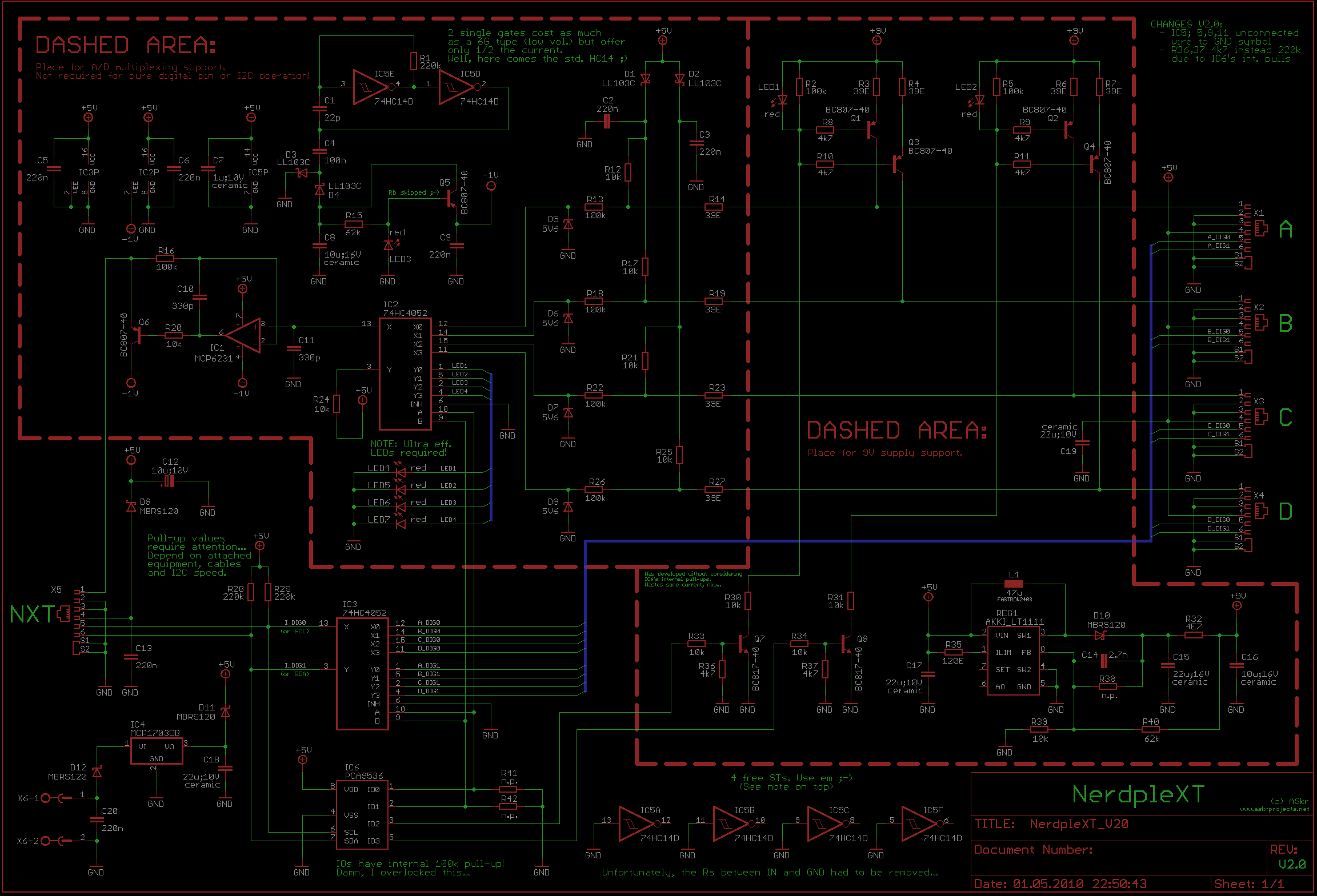
As a deterrent, we start off with the full-featured nerd version. Most will leave here. This safes a lot of traffic and keep the pages up ;)
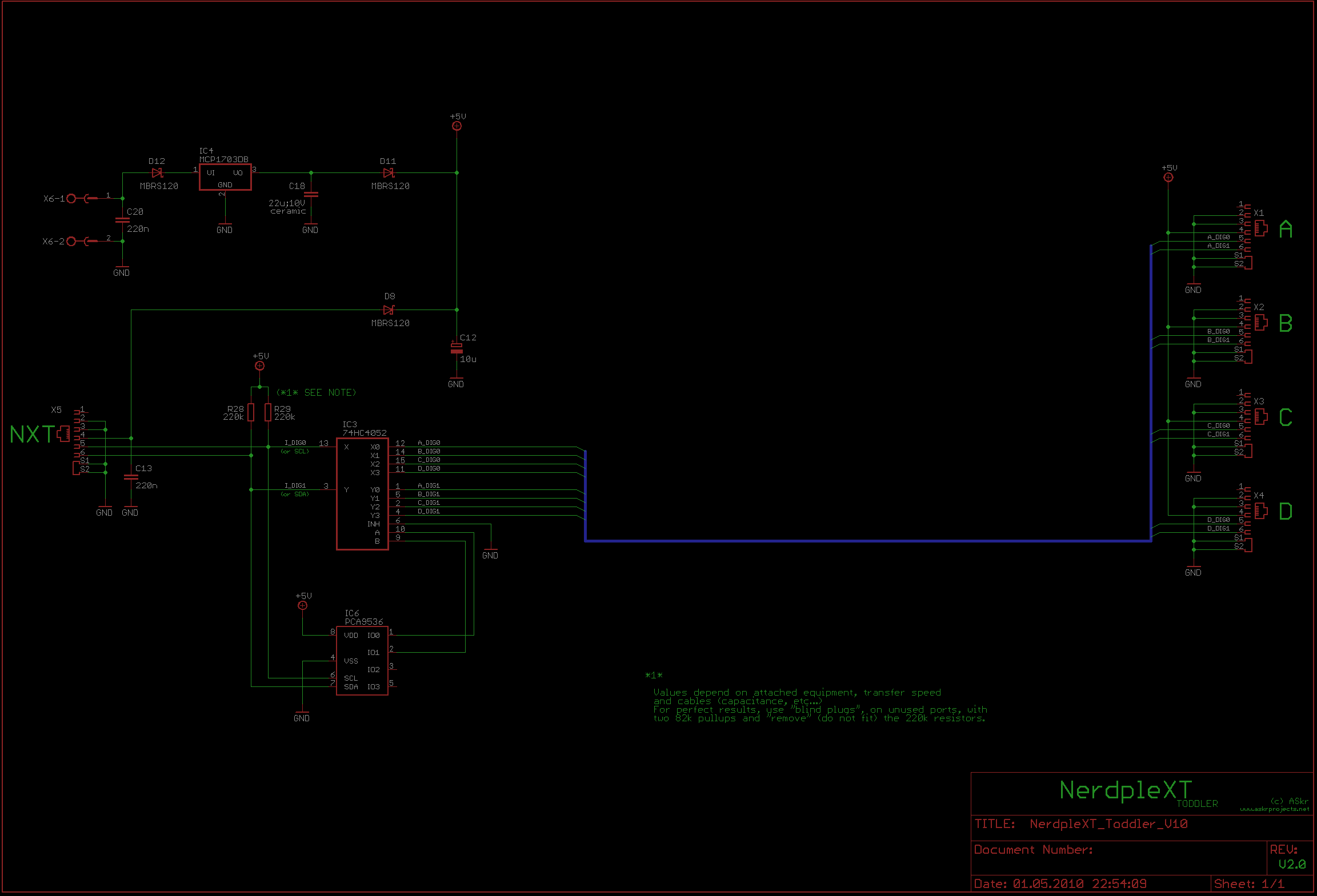
All the fancy stuff above can be reduced to a minimal, I2C-multiplexer toddler version:
Ok, let's focus on this basic circuit first...
The 74HC4052, if you do not know it already, is an analogue multiplexer. It connects pin X (Y) to any of the pins X0, X1, X2 or X3 (Y0,Y1,Y2,Y3), which can be selected by the control pins A and B:
|
B/A 0/0 0/1 1/0 1/1 |
selects X0,Y0 X1,Y1 X2,Y2 X3,Y3 |
The 74HC4052 (as well as its pure CMOS friend CD4052) really acts like a (poor) bidirectional 1-to-4 switch or relay. The current may take any direction. "Poor" means that the internal resistance can not compete against the mOhm values of a switch or a relay. A 74HC4052 has a typical, internal "ON" resistance of ~100 Ohms. (Though one could write much, much more on this topic, but I'll stop here. The DC behaviour is is all you need to know, so far ;-).
For any equipment attached to one of the ports A, B, C or D, the 74HC4052 is transparent. If the port is not selected, Xn and Yn will have a high impedance state and SDA and SCL are pulled up on the bus side (single Lego-sensor with internal termination or real I2C bus). If selected, any clock (SCL) or data-signal (SDA) will simply be fed through X<->Xn and Y<->Yn.
The port control is operated by a tiny and cheap PCA9536, a 4 bit I/O port device, attached to the NXT side of the I2C bus.
IO0 and IO1 are connected to the 74HC4052's A and B pins, controlling it directly.
On power-up, all 4 pins are configured as inputs, but are internally (PCA9536) pulled with 100k against Vdd. I overlooked
this while doing V1.0. As a result, R36 and R37 needed to be lowered down to 4k7 (from 220k), otherwise the 9V would be turned
on until the PCA9536 is configured (pins as outputs). For the same reason, R41 and R42 must not be fitted.
A note on I2C pull-up resistors:
Although I'm not going to explain the operation of the I2C bus, a "few" words on this:
An I2C bus needs pull-up resistors on both lines. These will create the "high" signal state. Any device, including the master, can not
source (put an active high state on any of the lines) but only sink current (open-collector or open-drain configuration), by pulling
the line down (to ground).
|
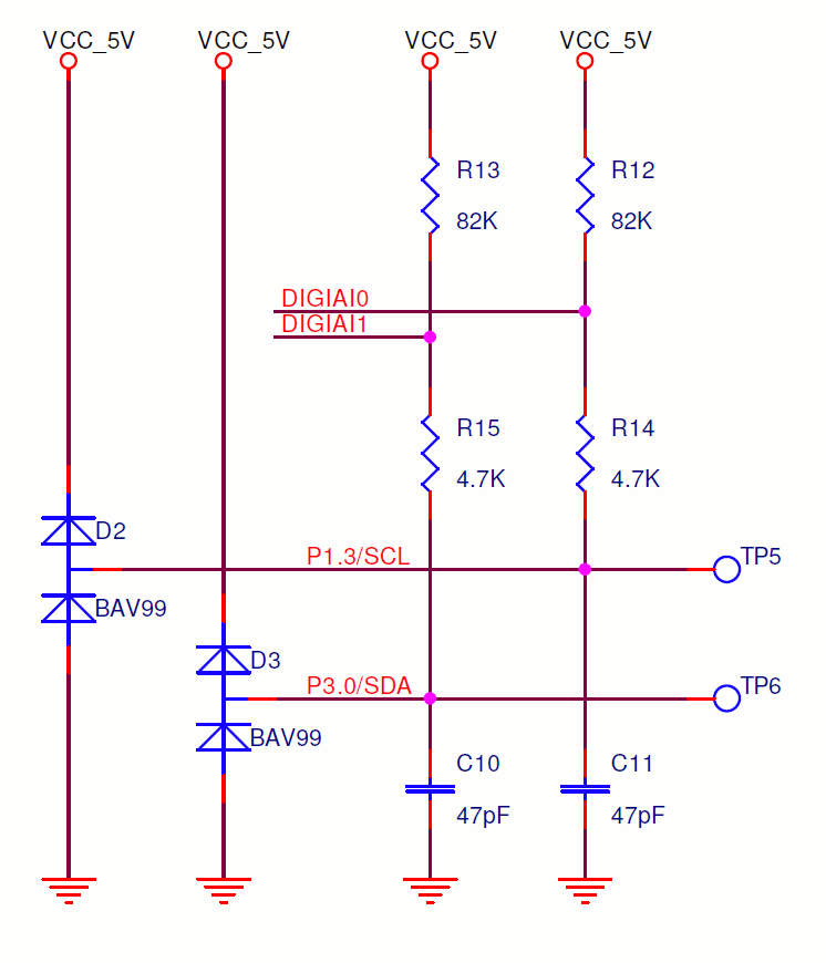
The image on the right depicts the internals of a NXT's I2C port. DIGIB0 is directly connected to the SAM7 processor, whereas
DIGIBI0 goes to pin 5 of sensor port #2. Having a processor's pins connected directly to an "output" (aka.: "the world outside") is
always a bad thing. The processor might (actually, one day it will...) get damaged by ESD
or behave strange because of other-weird-stuff coming in from
your black, flat
Fortunately, the Lego designers took care of this and added the usual protection: Notice that the 82k resistor is not fitted in the NXT (but it resides in every Lego I2C sensor, "outside" instead). |

|
Now imagine, the NXT's processor pulls DIGIB0 to ground. No matter if the sensor has the pull-up against 5V or 3.3V, the two resistors form a simple resistor divider. The voltage, that is seen by the sensor is:
"Usually" (...), all the I2C equipment operates with CMOS logic levels (NOTE: The English Wikipedia entry contains some severe errors. Because of this, the link points to the German article instead.) and even if your equipment uses TTL or whatever, the principle is the same:
The voltage needs to trip below a certain level, to generate a logical low state (the same, of course, applies to the high state which needs a voltage above a certain level).
For CMOS logic, for example, a low state is generated below ~1/3 of the supply voltage, whereas a high level will be valid for levels above ~2/3. The area beween those two is the "forbidden-zone". It might create a low OR a high state and can create excessive currents in the input stage (the only component capable of handling such levels is one that includes a hysteresis. E.g.: A Schmitt trigger).
For 5V supply, the boundary(!) value for a low state is ~1.5V. Usually, one would at least(!) need to half this value to be on the safe side under all circumstances. If we assume ~750mV, which still is a too high value (if you consider that we are talking about a dynamic behaviour, switching up and down and not a static DC signal!), we can calculate the minimal value of the external pull-up resistor, that will allow the sensor to detect a low state (in static DC applications!):
For any resistance below this value, a logic low level would never be reached (And if you really understand the above, you will notice that the voltage supply term cancels out of the formula. You will get the same result with a 3.3V supply and an adapted low logic-level ;-).
Usually, one would like to have the lowest possible value...
But wait, what is this:
Yes, but only statically. While the signal lines can be brought to ground very quickly (the transistors simply short the line to ground), the rising edge will suffer from the sum of all parasitic capacitances (cable, sensor, NXT).
The pull-up resistor needs to charge them all. Charging the line up to ~63%, the time-constant, calculates to:
Thus, increasing the resistance will slow down the rising-edge. Your one nice rectangular waveforms become triangles and the high-logic level might be reached too late. Thus, the processor recognizes a low-level instead and your communication will fail or bring up strange results...
Why is this all important?
If all four multiplexed ports are equipped with sensors or other I2C-conform devices (including the pull-ups), the two pull-up
resistors in the NerdpleXT hardware would not be required. But if only one port has no pulls and you once switch to this channel,
you're stuck and can never ever reach the internal PCA9536 again. All communication will fail due to the missing pull-up resistors.
To overcome this issue, you have two possibilities:
- fit the internal resistors
- use blind plugs with only pull-ups inside (no sensor or whatever else required)
These resistors will show up in parallel to the external ones, if a port with attached equipment is selected. The total resistance will be:
"total" = "internal" .. "external"
For the proposed 220k and externally attached 82k (Lego), the resulting resistance calculates to:
For whatever modification you make, whatever equipment you attach, make sure that the overall resistance does not fall below the critical level.
...
Damn. Did I say "a few words on pull-ups"?
There goes my time...
Back to the circuit:
Because four I2C ports, especially if whole busses are attached, may consume more power than the NXT can deliver, an external power
supply can be attached to X6. Five (fully charged) or six NiMH cells will work best (keep external voltage >6V).
This minimal version will operate with any I2C devices or busses except for the following:
- a second (or even more) I2C device with a device address of 1000001X (binary control byte)
- any Lego I2C sensor that additionally needs a 9V supply
Because the PCA9536 listens to all I2C traffic, a control byte with a value of 0x82 (or 0x83 for a read operation) will always activate it. No other device may share this address!
Although the 9V supply could be taken from a battery, we can do better:
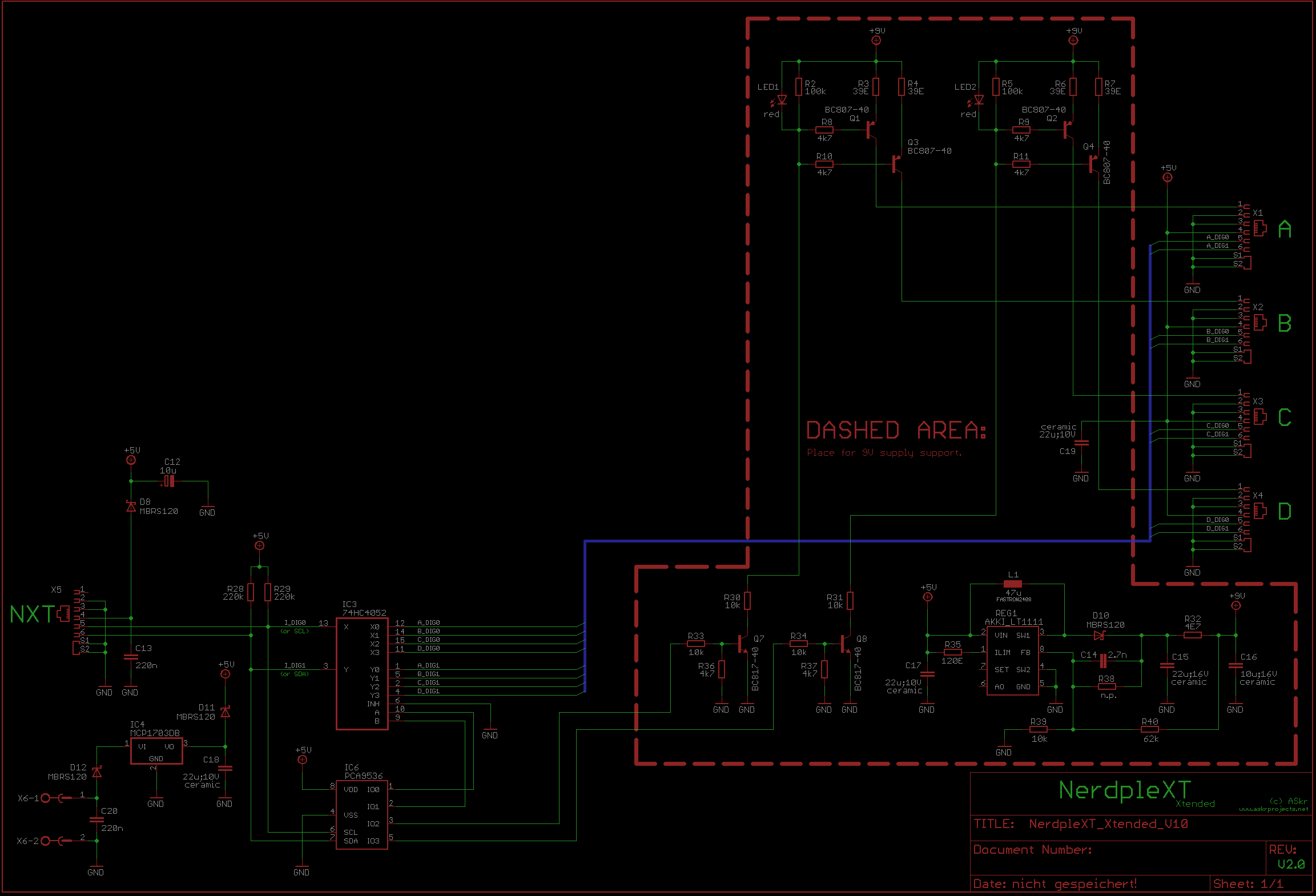
The Xtended version introduces two, current limited, power supplies. One, simultaneously powers port A+B, the other one C+D. They can be turned on or off via PCA9536 IO2 and IO3.
If one of the IO pins is high, the attached transistor Q7 or Q8 is activated and pulls R30 or R31 to ground. This turns on the transistors Q1, Q3 or Q2, Q4, which are configured as current sources, in conjunction with the red LEDs. The LED and the emitter resistors determine the current limitation, which operates independently on any of the four ports:
considering the additional voltage drop across Rb: ~20mA
Although the circuit could be dimensioned for lower currents, by increasing R30 and R31 (~730uA@10k), choosing a proper LED and high B transistors (though it will be hard to find anything much better than a BC807-40), the proposed dimensioning will work fine with a broad range of LEDs and transistors. Lower currents through R30 or R31, the "driving currents" for the upper transistors, additionally would require lower base resistor value, which reduces their decoupling effect on the adjacent current source and make the current limiting curve less sharp...
The 9V supply is created by a LT1111, a not-that-cheap boost regulator, which is always turned on. In quiescent state (no load),
it will consume a little less than 300uA.
I guess that's fair (at least for Lego equipment ;-).
While the DC feedback is derived from C16, the second filter stage and output, C14 helps reducing the ripple, which is caused by
the hysteresis of the LT1111's internal reference comparator (and the "giant" +30uF at the output ;), by coupling the switching
residuals into the feedback pin. Instead of shooting out several pulse packages at once, the LT1111 only fires a single one out now (little load).
The slow rising and current limited power output of the NXT is not sufficient to power up the LT1111. At least, if you have NerdpleXT already connected and turn on your NXT afterwards!
As a workaround, do one of the following:
- first turn on your NXT, and then plug in NerdpleXT
- use a battery pack (always recommended)
- try your luck with a LT1110
If none of the "port LEDs" (LED4-7) is on, the LT1111 hangs.
This power-on lock will be solved in V2.1 or V3.0...
Note: Excessive loads on the ports' 9V and 5V supply require a battery pack! The current output of the NXT's 5V supply (pin 4) is limited to a little more that ~220mA FOR ALL 4 SENSOR PORTS AND THE MOTOR ENCODERS TOGETHER (see here)!
Instead of mounting the LT1111 and peripherals, one could of course stick to a simple 9V battery...
Note: The 9V supply should be attached all the time! Otherwise, strange things may happen!
Because of the chosen design, the 9V supply is not transparent. Turning it on in the NXT (e.g. by activating the US or light sensor),
will not power the attached equipment. You have to do it by your own. Sensors, which need 9V supply, should not be mixed with ones
that do not need it, use the A/D pin (e.g. Lego switch) or may take damage...
But, it is safe to split them up: 9V on A+B, any other sensors go to C+D (or vice versa).
Because of D8, the internal "5V" supply, as well as the external A-D supply, will be ~4.4 - 4.0V, depending on load
(this circuit was developed for external 3.3V equipment, only!).
For a perfect 5.0V external supply, do the following:
- remove D8 (NerdpleXT will not be powered by the NXT anymore)
- remove D11
- solder a 0E (1206) resistor onto D11's pad
- use a battery pack
Now on to the all-in-one version:
Four 10k pull-up resistors (R12, R17, R21 and R25) simulate the NXT's A/D port (pin 1). A 100k and 5V6 Zener diode combination protect the following components against >5V voltages (e.g. if the 9V supply is turned on).
A second 74HC4052 (IC2), which uses the same channel selection like the one that sits on the I2C bus, feeds one of the four port's simulated A/D-pin signal into the MCP6231 (IC1), a low power OP, configured in non-inverted mode. The OP's output is boosted by a PNP transistor Q6 (BC807-40). R16 closes the feedback loop and C10 limits the bandwidth and prevents oscillations (Although the MCP6231 already has a GBP of 300kHz ;-).
Note: This configuration will even sink an enabled 9V supply down to ground (NXT pin 1). So, right now, it indeed is possible to have 9V activated AND read values from the A/D converter. Though this does not make that much sense: Pin 1, with 9V activated, has a current limitation of about 18mA. And this current will be flowing all the time! You are advised to keep the 9V turned off. But an accidental activation of the 9V supply won't do any harm to the circuit.
Normally, the PNP transistor would not be able to sink pin 1 down to ground. Because of its Ube, it would stop at ~650mV. To get past that limitation, the MCP6231, the attached transistor and the preceeding 4052 are operated by a negative voltage (appr. -1V), which is created by IC5, a 74HC14 and surrounding parts.
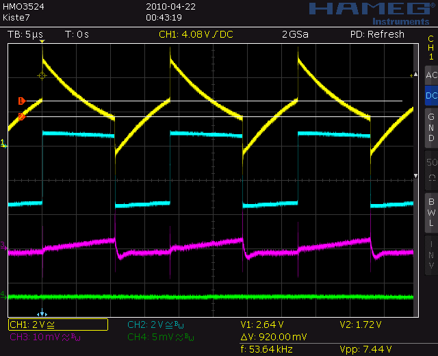
IC5, the 74HC14, operates as a free running oscillator in an "improved mode". The giant HC14 is in there, with four gates unused,
because two single gates cost the same but can only delive half the current.
Usually, C1, with a connection to ground and R1 would be sufficient to create an oscillation. This topology has the disadvantage,
that the voltage at pin 3 of the HC14 is always above 1/3 and below 2/3 of the supply voltage, right in the inner of the hysteresis
(in the screen shot below, this would be the area between the two cursors).
The negative voltage needed a limitation because the MCP6231, like most other rail-to-rail OPs, can only handle ~6V, with 7V as the
the absolute maximum specification...
Current consumption of this circuit is about ~200uA and it is able to supply ~5-7mA, depending on the HC14 (don't use Philips or
Lucky Goldstar [insider's joke] ;-)
At the very end, the remaining part of IC2 (74HC4052) is used to light up 1 of 4 LEDs (yes, red ones ;-) to indicate the activated port.
Note: I am using super-duper-efficient LEDs from Osram. They will light up brightly with only ~330uA! If you use standard, or even
worse LEDs, make sure to change R24, but remember that this current will flow all the time, possibly further reducing
the battery life...
the little test-layout...
|
... and an assembled PCB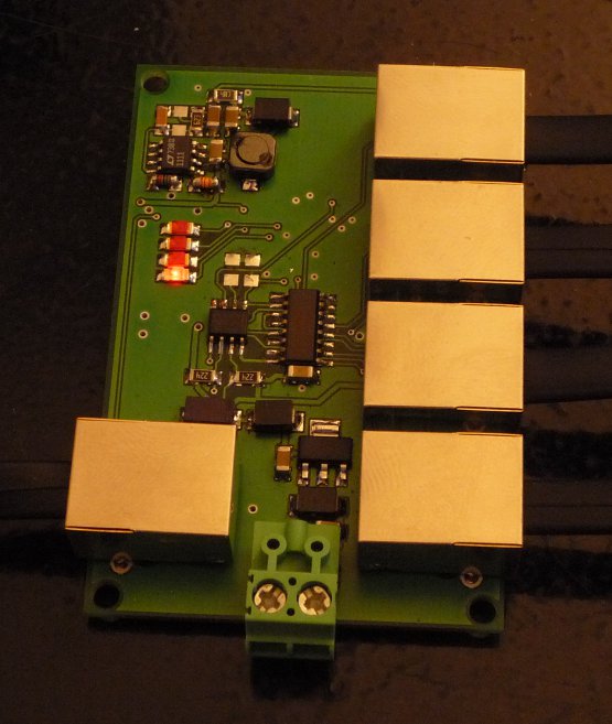
|
Software
A mini example of controlling NerdpleXT is available in the download section.
Download
NerdpleXT:
Includes:
- schematic (PDF)
- placement (PDF)
- BOM (TXT)
- layout, Eagle (BRD)
DOWNLOAD: NerdpleXT_V20-hard.zip V2.0; full featured nerd hardware-version
DOWNLOAD: NerdpleXT-soft.zip some pbLua routines to try
ASkr 04/2010 initial version


