pbRAM
A (data and function) memory upgrade for Lego-NXT.
ASkr 10/09:
New HW+SW for battery data retention (CR2332) online.
Rework instructions (easy!) available...
Features:
- general SPI interface for NXT
- easy to build (low pin count, single sided layout)
- no processor/programming necessary
- fair performance (considering native pbLua controlled pins ;)
- 3V lithium battery data retention
- transportable data and function memory
I needed a SPI interface for my NXTs _and_ I ran out of RAM.
Here's a simple method to combine two needs...
Can be used with a lot of SPI components. Drawback: You will lose one complete port...
So, you ran out of memory?
Not even unloading modules or using smaller storage classes helped?
You (may) have come to the right place...
Unfortunately, adding program memory to the NXT is not easy and may be impossible. Patching GCCs malloc() to use external interfaces may be a solution. This way, you could at least "outsource" the heap, where Lua stores most of its state. (But this is another project, we are currently working on...).
You still have the option to reload source code from flash via loadfile(), dofile(), etc..., or "unloading" released functions via a_function=nil.
If this all still does not help, adding additional, external data memory may do the trick.
And this is exactly, what this is all about...
Unlike my other solutions (authors note 8/2009: not published yet, due to chronic lack of time) pbCard and pbSerRAM, this one does not use a microcontroller.
We are going to hook up a Microchip 23K256
serial memory chip, via only two input-port pins.
Although its speed will not come up to the internal access times, having a supplementary data RAM of 32kB
size may be a fair compromise.
Well, I disagree, for the following three reasons
While the first and latter argument do not need any further investigation, I'll proof the second one:
Furthermore, the I2C send and receive routines can not handle more than 16 bytes at once. So, larger packets (tables) need
to be split up and sent each after another (which includes at least two additional address bytes for each 16-byte
packet)... While this is unimportant for random access of a single byte, it is a drawback for storing larger
chunks of memory, like functions.
Apart from that, Ramtron's FRAMs and Microchip's 23k256 are "pretty equal" (concerning aspects of the protocol and functionality).
And well, did I already mention the "fun part"? 8-)
ASkr 12/2009:
Some readers claimed that, except for having a SPI interface, an I2C solution, probably with a
Ramtron FRAM chip,
would be an easier way of adding memory to the (pbLualized) NXT.
(and leave the battery as well as I2Cs bus capability unconsidered, hehe ;-):
(Which does not mean the FRAM isn't a very promising and interesting future candidate...
I bought a tray of FRAM chips ;-)
At a glance, nxt.I2CSendData() and nxt.I2CRecvData() are all you need. A closer look at their functionality
requires this, as an absolute minimum, only for the lower sending and receiving part:
Because the I2C routines are interrupt driven, you will need the complete set of checking for its availability
and state. If you skip certain checks or procedures (e.g. leave on timeout), your application may hang if you
pull off the hardware...
cI2CTIMEOUT  = 250     -- in ms
cI2CREPDELAY = 10      -- delay between multiple tries (in ms)

function utilI2Comm(port, sCmd, rBytes)
  local tim=nxt.TimerRead()
  local i
  local sTmp=""

  -- wait for I2C to become ready
  while ({nxt.I2CGetStatus(port)})[1] ~= 0 do
    if nxt.TimerRead() > tim+cI2CTIMEOUT then
      return nil
    end
  end

  sTmp=string.char(unpack(sCmd))

  tim=nxt.TimerRead()

  -- try to send or receive until timeout occurs
  while 1
  do

    -- send string
    nxt.I2CSendData(port,sTmp,rBytes)

    while 1 do
      local a,b,c=nxt.I2CGetStatus(port)

      if a==0 then
        if rBytes<1 then
          return {} -- no answer required
        else
          sTmp=nxt.I2CRecvData(port,rBytes)
          local tRet={}
          local i
          for i=1,rBytes do
            table.insert(tRet,string.byte(sTmp,i))
          end
          return tRet
        end --else return data
      end -- end if all OK

      -- check for timeout
      if nxt.TimerRead() > tim+cI2CTIMEOUT  then
        return nil --timeout
      end

      -- check for error (e.g.: missing ACKs...)
      if b==255 then
        utilWait(cI2CREPDELAY)
        break
      end

    end -- while status pending

  end -- while forever

  return nil

end -- function
Writing your own I2C routines is strongly recommended if you wish to get past the limits.
23k256
FM24L256
max speed
20 MHz
1 MHz
standby current
4 uA
12 uA
op. current (1MHz)
3 mA
600 uA (*2*)
auto increment
yes
yes
address roll over
yes
yes
cost (*3*)
1 EUR
10 EUR
(*2*) SCL toggling; other inputs Vss or Vdd
(*3*) Farnell, Germany, 12/2009
Functional Description
The 23K256 has a SPI interface, hence we would need:- CS, a chip select
- SI, serial data in
- SO, serial data out
- SCK, data clock.
A NXT input port has 3 pins available:
- pin 1 -> high voltage supply and A/D converter, mutually exclusive
- pin 5 -> dig0, IO
- pin 6 -> dig1, IO
As it turned out, pin 1 can not be used (even if equipped with a level converter), because it
only can be switched within (up to) 35ms. Far too slow!
So, we actually have no more than 2 pins per port. Sacrificing two complete ports is not an option!
Do not even think about that ;-)
Well, how do we control 4 lines via only 2 pins?
The 23K256 has no synchronous bidirectional (aka.: "full duplex") mode. SI and SO are always active one
at a time.
=> can be combined;
We still need /CS.
Having it pulled down all the time will not work. Besides its function as a pure "chip select",
it internally resets the state of the chip. Without that, it never would accept any new address or set SO to
high impedance state after data was send out.
But we can, indeed, combine SCK and /CS (pin 5, dig0):
Note: Old HW, only for functional description!
Click schematic for better resolution.

The quiescent condition is having (NXT) pin 5 high, hence 23K256's /CS and SCK are high too.
A negative pulse on (NXT) pin 5 will not only pull (23K256) SCK low but also immediately discharge C3 via D1
and clear /CS (via IC2 F+A).
Data is clocked in (or out, respectively) on the rising edge of SCK. While (NXT) pin 5 rises, C3 will retain
its low state for (a little less then) t=R3*C3 = ~450us.
The next negative edge of SCK will instantly reset the time constant again.
After all data is clocked in/out, /CS will follow SCK high, after about ~450us. Inserting a 1ms delay in the source code (the shortest available timer handled timespan) is essential.
|
Writing a 32 bit value (a pbLua "number" variable) takes about 6ms. Click to enlarge. 
|
Reading a 32 bit value takes a little bit longer: ~9ms. Click to enlarge. 
|
The two, big (~1.4V) spikes on the R/C SCK line (red) result from any of pbLua's interrupt routines.
ASkr 8/2009:
As of pbLua v18a, it now has a function to disable the internal ISR: nxt.DisableNXT().
Great! All spikes are gone and we gained a few microseconds ;-)
ASkr 9/2009:
To maintain the direction of the pins (in or out), just put a "nil" in nxt.InputSetState() wherever you
like to maintain the input state.
Mhh, what about yellow instead of an annoying green?
And another one.
As of pbLua v18c, calls to nxt.InputSetState() have no influence on the direction of the pins
(In older versions, any call to ...SetState() changed the pin direction to output immediately),
so the additional call to nxt.InputSetDir() could be omitted.
With nxt.DisableNXT(); Writing and reading an 8 and a 32 bit value.
2.9ms / 3.2ms /4.7ms / 6.1ms
Click to enlarge.

Hardware
Note:The new BDR (battery data retention) edition is not software compatible with the old one!
While creating the first version, I never thought about having a battery on the PCB, hence I did not care about the NXT internal pull-down resistors (and the clamping parasitic diodes in the SAM7) and the lowered SCK line kept the 23K256 enabled.
This used up to ~1.5mA, while the NXT was attached but turned of.
The new HW has an inverted SCK line to keep the CS pin of the 23K256 high.
The battery quiescent current of the circuit is about ~1.8uA. Considering a typical CR2032 battery, with a capacity of 150mAh, the data could (theoretically ;-) be stored for 9.5 years...
Note: To achieve this "low" (low is something different ;) current, do NOT choose any other than the recommended
voltage regulator (Seiko S817). It has a quiescent current of 1uA! You can not put any "LM..." or whatever in there!
As a alternative, Ricoh as well as Torex, offer fit, form and function compatible devices...
ASkr 12/09:
Some asked if the battery is required for operation.
No, it isn't! You can simply leave it out... It won't affect the circuit or its functionality.
Rework instructions for those who already built the original version:
Click to enlarge.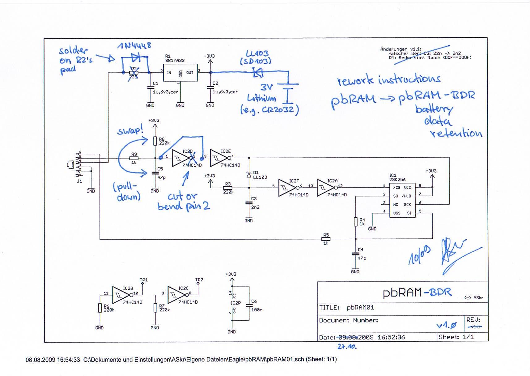
|
Click to enlarge.
|
a little larger than before...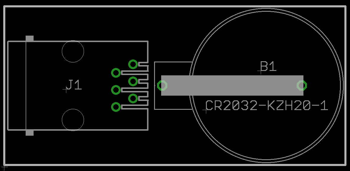
|
Just a quick change; Could be better...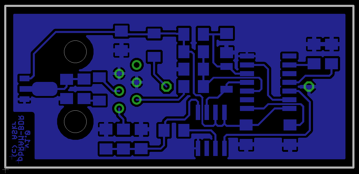
|
Usage
ASkr 10/09:Temporarily deleted. Needs some updates for BDR-edition...
In the meantime, you can download a pbLua sample application below (though this does not contain any code to store or recall pbLua functions...).
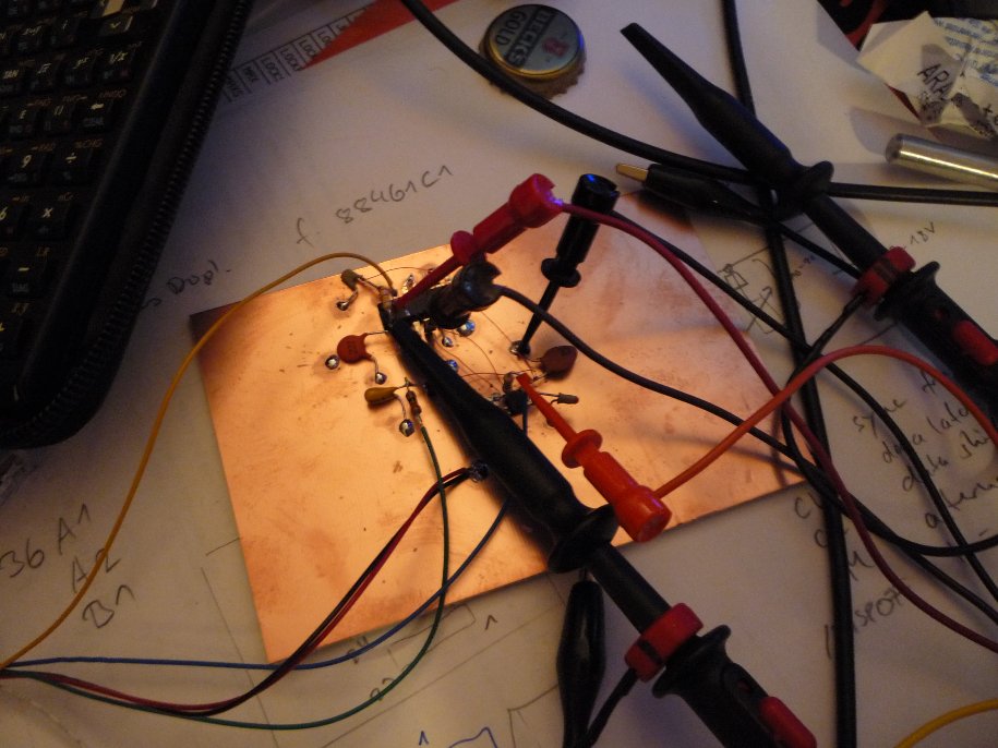
Some useless pics, as usual ;)
Need more RAM
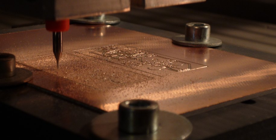
Warm the iron...
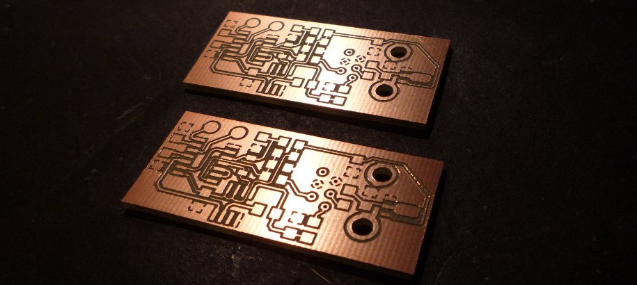
As usual, some SMD components staunchly refused being retrieved...
No problem, we simply use their through hole variant and memorize the next project:
Restore order and mill lockable(!) boxes. Damn!
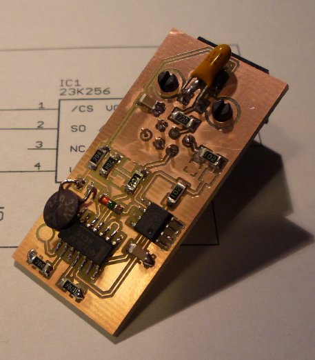
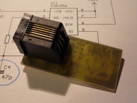
a reworked pbRAM for BDR operation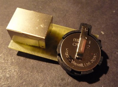
|
still some THs on there ;)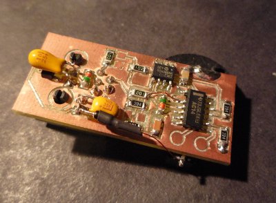
|
Download
pbRAM-BDR:
Includes:
- schematic (PDF)
- placement (PDF)
- layout, eagle (BRD)
- stinky BOM (TXT)
- sample pbLua application (TXT)
DOWNLOAD: pbram-bdr.zip
DOWNLOAD: pbram-bdr-code.zip
pbRAM (old, original version):
Includes:
- schematic (PDF)
- placement (PDF)
- layout, eagle (BRD)
- sample pbLua application (TXT)
DOWNLOAD: pbram.zip
DOWNLOAD: pbram-code.zip
ASkr 06/2009
ASkr 10/2009

